- 您现在的位置:买卖IC网 > Sheet目录3870 > PIC18LF4553T-I/ML (Microchip Technology)IC PIC MCU FLASH 16KX16 44QFN
2009 Microchip Technology Inc.
DS39887C-page 35
PIC18F2458/2553/4458/4553
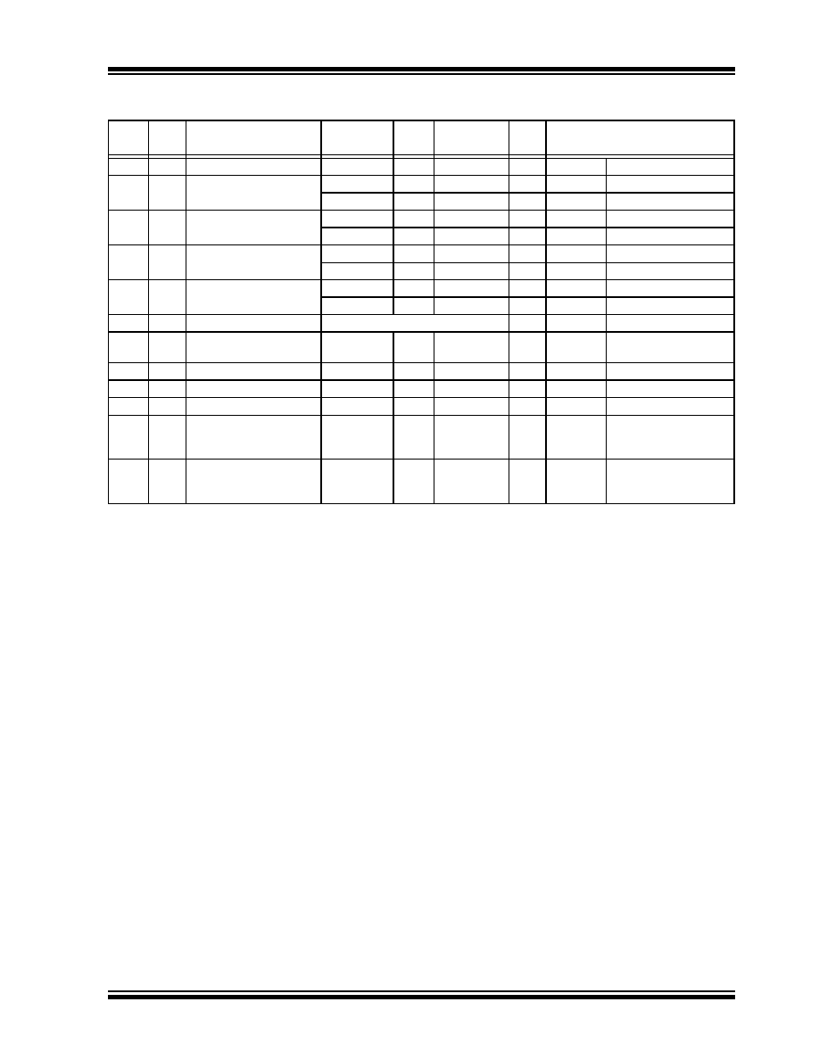
TABLE 4-1:
A/D CONVERTER CHARACTERISTICS: PIC18F2458/2553/4458/4553 (INDUSTRIAL)
PIC18LF2458/2553/4458/4553 (INDUSTRIAL)
Param
No.
Sym
Characteristic
Min
Typ
Max
Units
Conditions
A01
NR
Resolution
—
12
bit
ΔVREF ≥ 3.0V
A03
EIL
Integral Linearity Error
—
±1
±2.0
LSB
VDD = 3.0V
ΔVREF ≥ 3.0V
——
±2.0
LSB
VDD = 5.0V
A04
EDL
Differential Linearity Error
—
±1
+1.5/-1.0
LSB
VDD = 3.0V
ΔVREF ≥ 3.0V
——
+1.5/-1.0
LSB
VDD = 5.0V
A06
EOFF
Offset Error
—
±1
±5
LSB
VDD = 3.0V
ΔVREF ≥ 3.0V
——
±3
LSB
VDD = 5.0V
A07
EGN
Gain Error
—
±1
±1.25
LSB
VDD = 3.0V
ΔVREF ≥ 3.0V
——
±2.00
LSB
VDD = 5.0V
A10
—
Monotonicity
Guaranteed(1)
—VSS
≤ VAIN ≤ VREF
A20
ΔVREF Reference Voltage Range
(VREFH – VREFL)
3—
VDD – VSS
V
For 12-bit resolution
A21
VREFH Reference Voltage High
VSS + 3.0V
—
VDD + 0.3V
V
For 12-bit resolution
A22
VREFL Reference Voltage Low
VSS – 0.3V
—
VDD – 3.0V
V
For 12-bit resolution
A25
VAIN
Analog Input Voltage
VREFL
—VREFH
V
A30
ZAIN
Recommended
Impedance of Analog
Voltage Source
——
2.5
k
Ω
A50
IREF
VREF Input Current(2)
—
5
150
μA
During VAIN acquisition.
During A/D conversion
cycle.
Note 1:
The A/D conversion result never decreases with an increase in the input voltage and has no missing codes.
2:
VREFH current is from the RA3/AN3/VREF+ pin or VDD, whichever is selected as the VREFH source.
VREFL current is from the RA2/AN2/VREF-/CVREF pin or VSS, whichever is selected as the VREFL source.
发布紧急采购,3分钟左右您将得到回复。
相关PDF资料
PIC18LF2553T-I/SO
IC PIC MCU FLASH 16KX16 28SOIC
PIC18LF2221T-I/SS
IC PIC MCU FLASH 2KX16 28SSOP
PIC16F648A-I/P
IC MCU FLASH 4KX14 EEPROM 18DIP
PIC18F96J65T-I/PF
IC PIC MCU FLASH 48KX16 100TQFP
PIC16CE623-20/P
IC MCU OTP 512X14 EE COMP 18DIP
PIC24FJ16MC102-I/SO
IC MCU 16BIT 16KB FLASH 28SOIC
DSPIC33FJ16GP102-I/SO
IC DSC 16BIT 16KB 28SOIC
PIC16C57C-04/SO
IC MCU OTP 2KX12 28SOIC
相关代理商/技术参数
PIC18LF4553T-I/PT
功能描述:8位微控制器 -MCU 32KB FLSH 2048 RAM FSUSB 2.0 12B ADC RoHS:否 制造商:Silicon Labs 核心:8051 处理器系列:C8051F39x 数据总线宽度:8 bit 最大时钟频率:50 MHz 程序存储器大小:16 KB 数据 RAM 大小:1 KB 片上 ADC:Yes 工作电源电压:1.8 V to 3.6 V 工作温度范围:- 40 C to + 105 C 封装 / 箱体:QFN-20 安装风格:SMD/SMT
PIC18LF4580-I/ML
功能描述:8位微控制器 -MCU 32 KB FL 1536 RAM 36 I/O RoHS:否 制造商:Silicon Labs 核心:8051 处理器系列:C8051F39x 数据总线宽度:8 bit 最大时钟频率:50 MHz 程序存储器大小:16 KB 数据 RAM 大小:1 KB 片上 ADC:Yes 工作电源电压:1.8 V to 3.6 V 工作温度范围:- 40 C to + 105 C 封装 / 箱体:QFN-20 安装风格:SMD/SMT
PIC18LF4580-I/P
功能描述:8位微控制器 -MCU 32 KB FL 1536 RAM 36 I/O RoHS:否 制造商:Silicon Labs 核心:8051 处理器系列:C8051F39x 数据总线宽度:8 bit 最大时钟频率:50 MHz 程序存储器大小:16 KB 数据 RAM 大小:1 KB 片上 ADC:Yes 工作电源电压:1.8 V to 3.6 V 工作温度范围:- 40 C to + 105 C 封装 / 箱体:QFN-20 安装风格:SMD/SMT
PIC18LF4580-I/PT
功能描述:8位微控制器 -MCU 32 KB FL 1536 RAM 36 I/O RoHS:否 制造商:Silicon Labs 核心:8051 处理器系列:C8051F39x 数据总线宽度:8 bit 最大时钟频率:50 MHz 程序存储器大小:16 KB 数据 RAM 大小:1 KB 片上 ADC:Yes 工作电源电压:1.8 V to 3.6 V 工作温度范围:- 40 C to + 105 C 封装 / 箱体:QFN-20 安装风格:SMD/SMT
PIC18LF4580T-I/ML
功能描述:8位微控制器 -MCU 32 KB FL 1536 RAM 36 I/O RoHS:否 制造商:Silicon Labs 核心:8051 处理器系列:C8051F39x 数据总线宽度:8 bit 最大时钟频率:50 MHz 程序存储器大小:16 KB 数据 RAM 大小:1 KB 片上 ADC:Yes 工作电源电压:1.8 V to 3.6 V 工作温度范围:- 40 C to + 105 C 封装 / 箱体:QFN-20 安装风格:SMD/SMT
PIC18LF4580T-I/PT
功能描述:8位微控制器 -MCU 32 KB FL 1536 RAM 36 I/O RoHS:否 制造商:Silicon Labs 核心:8051 处理器系列:C8051F39x 数据总线宽度:8 bit 最大时钟频率:50 MHz 程序存储器大小:16 KB 数据 RAM 大小:1 KB 片上 ADC:Yes 工作电源电压:1.8 V to 3.6 V 工作温度范围:- 40 C to + 105 C 封装 / 箱体:QFN-20 安装风格:SMD/SMT
PIC18LF4585-I/ML
功能描述:8位微控制器 -MCU 48KB 3328 RAM w/ECAN RoHS:否 制造商:Silicon Labs 核心:8051 处理器系列:C8051F39x 数据总线宽度:8 bit 最大时钟频率:50 MHz 程序存储器大小:16 KB 数据 RAM 大小:1 KB 片上 ADC:Yes 工作电源电压:1.8 V to 3.6 V 工作温度范围:- 40 C to + 105 C 封装 / 箱体:QFN-20 安装风格:SMD/SMT
PIC18LF4585-I/P
功能描述:8位微控制器 -MCU 48KB 3328 RAM w/ECAN RoHS:否 制造商:Silicon Labs 核心:8051 处理器系列:C8051F39x 数据总线宽度:8 bit 最大时钟频率:50 MHz 程序存储器大小:16 KB 数据 RAM 大小:1 KB 片上 ADC:Yes 工作电源电压:1.8 V to 3.6 V 工作温度范围:- 40 C to + 105 C 封装 / 箱体:QFN-20 安装风格:SMD/SMT